The semiconductor industry has reached a pivotal milestone in the race to sustain the explosive growth of artificial intelligence. As of early 2026, the formalization of the "One Team" alliance between SK Hynix (KRX: 000660) and Taiwan Semiconductor Manufacturing Company (NYSE: TSM) has fundamentally restructured how high-performance memory is designed and manufactured. This collaboration marks the transition to HBM4, the sixth generation of High Bandwidth Memory, which aims to dissolve the data-transfer bottlenecks that have long hampered the performance of the world’s most advanced Large Language Models (LLMs).
The immediate significance of this development lies in the unprecedented integration of logic and memory. For the first time, HBM is moving away from being a "passive" storage component to an "active" participant in AI computation. By leveraging TSMC’s advanced logic nodes for the base die of SK Hynix’s memory stacks, the alliance is providing the necessary infrastructure for NVIDIA’s (NASDAQ: NVDA) next-generation Rubin architecture, ensuring that the next wave of trillion-parameter models can operate without the crippling latency of previous hardware generations.
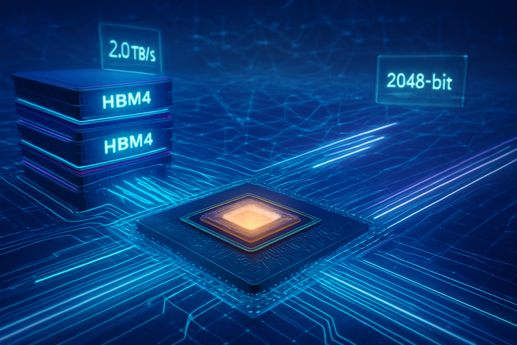
The 2048-Bit Leap: Redefining the HBM Architecture
The technical specifications of HBM4 represent the most aggressive architectural shift since the technology's inception. While generations HBM2 through HBM3e relied on a 1024-bit interface, HBM4 doubles the bus width to a massive 2048-bit interface. This "wider pipe" allows for a dramatic increase in data throughput—targeting per-stack bandwidths of 2.0 TB/s to 2.8 TB/s—without requiring the extreme clock speeds that lead to thermal instability and excessive power consumption.
Central to this advancement is the logic die transition. Traditionally, the base die (the bottom-most layer of the HBM stack) was manufactured using the same DRAM process as the memory cells. In the HBM4 era, SK Hynix has outsourced the production of this base die to TSMC, utilizing their 5nm and 12nm logic nodes. This allows for complex routing and "active" power management directly within the memory stack. To accommodate 16-layer (16-Hi) stacks within the strict 775 µm height limit mandated by JEDEC, SK Hynix has refined its Mass Reflow Molded Underfill (MR-MUF) process, thinning individual DRAM wafers to approximately 30 µm—roughly half the thickness of a human hair.
Early reactions from the AI research community have been overwhelmingly positive, with experts noting that the transition to a 2048-bit interface is the only viable path forward for "scaling laws" to continue. By allowing the memory to act as a co-processor, HBM4 can perform basic data pre-processing and routing before the information even reaches the GPU. This "compute-in-memory" approach is seen as a definitive answer to the thermal and signaling challenges that threatened to plateau AI hardware performance in late 2025.
Strategic Realignment: How the Alliance Reshapes the AI Market
The SK Hynix and TSMC alliance creates a formidable competitive barrier for other memory giants. By locking in TSMC’s world-leading logic processes and Chip-on-Wafer-on-Substrate (CoWoS) packaging, SK Hynix has secured its position as the primary supplier for NVIDIA’s upcoming Rubin R100 GPUs. This partnership effectively creates a "custom HBM" ecosystem where memory is co-designed with the AI accelerator itself, rather than being a commodity part purchased off the shelf.
Samsung Electronics (KRX: 005930), the world’s largest memory maker, is responding with its own "turnkey" strategy. Leveraging its internal foundry and packaging divisions, Samsung is aggressively pushing its 1c DRAM process and "Hybrid Bonding" technology to compete. Meanwhile, Micron Technology (NASDAQ: MU) has entered the HBM4 fray by sampling stacks with speeds of 11 Gbps, targeting a significant share of the mid-to-high-end AI server market. However, the SK Hynix-TSMC duo remains the "gold standard" for the ultra-high-end segment due to their deep integration with NVIDIA’s roadmap.
For AI startups and labs, this development is a double-edged sword. While HBM4 provides the raw power needed for more efficient inference and faster training, the complexity and cost of these components may further consolidate power among the "hyperscalers" like Microsoft and Google, who have the capital to secure early allocations of these expensive stacks. The shift toward "Custom HBM" means that generic memory may no longer suffice for cutting-edge AI, potentially disrupting the business models of smaller chip designers who lack the scale to enter complex co-development agreements.
Breaking the "Memory Wall" and the Future of LLMs
The development of HBM4 is a direct response to the "Memory Wall"—a long-standing phenomenon where the speed of data transfer between memory and processors fails to keep pace with the increasing speed of the processors themselves. In the context of LLMs, this bottleneck is most visible during the "decode" phase of inference. When a model like GPT-5 or its successors generates text, it must read massive amounts of model weights from memory for every single token produced. If the bandwidth is too narrow, the GPU sits idle, leading to high latency and exorbitant operating costs.
By doubling the interface width and integrating logic, HBM4 allows for much higher "tokens per second" in inference and shorter training epochs. This fits into a broader trend of "architectural specialization" in the AI landscape. We are moving away from general-purpose computing toward a world where every millimeter of the silicon interposer is optimized for tensor operations. HBM4 is the first generation where memory truly "understands" the data it holds, managing its own thermal profile and data routing to maximize the throughput of the connected GPU.
Comparisons are already being drawn to the introduction of the first HBM by AMD and Hynix in 2013, which revolutionized high-end graphics. However, the stakes for HBM4 are exponentially higher. This is not just about better graphics; it is the physical foundation upon which the next generation of artificial general intelligence (AGI) research will be built. The potential concern remains the extreme difficulty of manufacturing these 16-layer stacks, where a single defect in one of the thousands of micro-bumps can render the entire $10,000+ assembly useless.
The Road to 16-Layer Stacks and Hybrid Bonding
Looking ahead to the remainder of 2026, the focus will shift from the initial 12-layer HBM4 stacks to the much-anticipated 16-layer versions. These stacks are expected to offer capacities of up to 64GB per stack, allowing an 8-stack GPU configuration to boast over half a terabyte of high-speed memory. This capacity leap is essential for running trillion-parameter models entirely in-memory, which would drastically reduce the energy consumption associated with moving data across different hardware nodes.
The next technical frontier is "Hybrid Bonding" (copper-to-copper), which eliminates the need for solder bumps between memory layers. While SK Hynix is currently leading with its advanced MR-MUF process, Samsung is betting heavily on Hybrid Bonding to achieve even thinner stacks and better thermal performance. Experts predict that while HBM4 will start with traditional bonding methods, a "Version 2" of HBM4 or an early HBM5 will likely see the industry-wide adoption of Hybrid Bonding as the physical limits of wafer thinning are reached.
The immediate challenge for the SK Hynix and TSMC alliance will be yield management. Mass producing a 2048-bit interface with 16 layers of thinned DRAM is a manufacturing feat of unprecedented complexity. If yields stabilize by Q3 2026 as projected, we can expect a significant acceleration in the deployment of "Agentic AI" systems that require the low-latency, high-bandwidth environment that only HBM4 can provide.
A Fundamental Shift in the History of Computing
The emergence of HBM4 through the SK Hynix and TSMC alliance represents a paradigm shift from memory being a standalone component to an integrated sub-system of the AI processor. By shattering the 1024-bit barrier and embracing logic-integrated "Active Memory," these companies have cleared a path for the next several years of AI scaling. The shift from passive storage to co-processing memory is one of the most significant changes in computer architecture since the advent of the Von Neumann model.
In the coming months, the industry will be watching for the first "qualification" milestones of HBM4 with NVIDIA’s Rubin platform. The success of these tests will determine the pace at which the next generation of AI services can be deployed globally. As we move further into 2026, the collaboration between memory manufacturers and foundries will likely become the standard model for all high-performance silicon, further intertwining the fates of the world’s most critical technology providers.
This content is intended for informational purposes only and represents analysis of current AI developments.
TokenRing AI delivers enterprise-grade solutions for multi-agent AI workflow orchestration, AI-powered development tools, and seamless remote collaboration platforms.
For more information, visit https://www.tokenring.ai/.