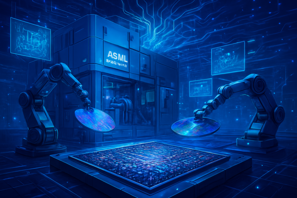
As of late 2025, the semiconductor industry has officially crossed the threshold into the "Angstrom Era," a pivotal transition that marks the end of the nanometer-scale naming convention and the beginning of atomic-scale precision. This shift is being driven by the deployment of High-Numerical Aperture (High-NA) Extreme Ultraviolet (EUV) lithography, a technological feat centered around ASML (NASDAQ: ASML) and its massive TWINSCAN EXE:5200B scanners. These machines, which now command a staggering price tag of nearly $400 million each, are the essential "printing presses" for the next generation of 1.8nm and 1.4nm chips that will power the increasingly demanding AI models of the late 2020s.
The immediate significance of this development cannot be overstated. While the previous generation of EUV tools allowed the industry to reach the 3nm threshold, the move to 1.8nm (Intel 18A) and beyond requires a level of resolution that standard EUV simply cannot provide without extreme complexity. By increasing the numerical aperture from 0.33 to 0.55, ASML has enabled chipmakers to print features as small as 8nm in a single pass. This breakthrough is the cornerstone of Intel’s (NASDAQ: INTC) aggressive strategy to reclaim the process leadership crown, signaling a massive shift in the competitive landscape between the United States, Taiwan, and South Korea.
The Technical Leap: From 0.33 to 0.55 NA
The transition to High-NA EUV represents the most significant change in lithography since the introduction of EUV itself. At the heart of the ASML TWINSCAN EXE:5200B is a completely redesigned optical system. Standard EUV tools use a 0.33 NA lens, which, while revolutionary, hit a physical limit when trying to print features for nodes below 2nm. To achieve the necessary density, manufacturers were forced to use "multi-patterning"—essentially printing a single layer multiple times to create finer lines—which increased production time, lowered yields, and spiked costs. High-NA EUV solves this by using a 0.55 NA system, allowing for a nearly threefold increase in transistor density and reducing the number of critical mask steps from over 40 to single digits.
However, this leap comes with immense technical challenges. High-NA scanners utilize an "anamorphic" lens design, which means they magnify the image differently in the horizontal and vertical directions. This results in a "half-field" exposure, where the scanner only prints half the area of a standard mask at once. To overcome this, the industry has had to master "mask stitching," a process where two exposures are perfectly aligned to create a single large chip. This required a massive overhaul of Electronic Design Automation (EDA) tools from companies like Synopsys (NASDAQ: SNPS) and Cadence (NASDAQ: CDNS), which now use AI-driven algorithms to ensure layouts are "stitching-aware."
The technical specifications of the EXE:5200B are equally daunting. The machine weighs over 150 tons and requires two Boeing 747s to transport. Despite its size, it maintains a throughput of 175 to 200 wafers per hour, a critical metric for high-volume manufacturing (HVM). Furthermore, because the 8nm resolution requires incredibly thin photoresists, the industry has shifted toward Metal Oxide Resists (MOR) and dry-resist technology, pioneered by companies like Applied Materials (NASDAQ: AMAT), to prevent the collapse of the tiny transistor structures during the etching process.
A Divided Industry: Strategic Bets on the Angstrom Era
The adoption of High-NA EUV has created a fascinating strategic divide among the world's top chipmakers. Intel has taken the most aggressive stance, positioning itself as the "first-mover" in the High-NA space. By late 2025, Intel has successfully integrated High-NA tools into its 18A (1.8nm) production line to optimize critical layers and is using the technology as the foundation for its upcoming 14A (1.4nm) node. This "all-in" bet is designed to leapfrog TSMC (NYSE: TSM) and prove that Intel's RibbonFET (Gate-All-Around) and PowerVia (backside power delivery) architectures are superior when paired with the world's most advanced lithography.
In contrast, TSMC has adopted a more cautious, "prudent" path. The Taiwanese giant has opted to skip High-NA for its A16 (1.6nm) and A14 (1.4nm) nodes, instead relying on "hyper-multi-patterning" with standard 0.33 NA EUV tools. TSMC’s leadership argues that the cost and complexity of High-NA do not yet justify the benefits for their current customer base, which includes Apple and Nvidia. TSMC expects to wait until the A10 (1nm) node, likely around 2028, to fully embrace High-NA. This creates a high-stakes experiment: can Intel’s technological edge overcome TSMC’s massive scale and proven manufacturing efficiency?
Samsung Electronics (KRX: 005930) has taken a middle-ground approach. While it took delivery of an R&D High-NA tool (the EXE:5000) in early 2025, it is focusing its commercial High-NA efforts on its SF1.4 (1.4nm) node, slated for 2027. This phased adoption allows Samsung to learn from the early challenges faced by Intel while ensuring it doesn't fall as far behind as TSMC might if Intel’s bet pays off. For AI startups and fabless giants, this split means choosing between the "bleeding edge" performance of Intel’s High-NA nodes or the "mature reliability" of TSMC’s standard EUV nodes.
The Broader AI Landscape: Why Density Matters
The transition to the Angstrom Era is fundamentally an AI story. As large language models (LLMs) and generative AI applications become more complex, the demand for compute power and energy efficiency is growing exponentially. High-NA EUV is the only path toward creating the ultra-dense GPUs and specialized AI accelerators (NPUs) required to train the next generation of models. By packing more transistors into a smaller area, chipmakers can reduce the physical distance data must travel, which significantly lowers power consumption—a critical factor for the massive data centers powering AI.
Furthermore, the introduction of "Backside Power Delivery" (like Intel’s PowerVia), which is being refined alongside High-NA lithography, is a game-changer for AI chips. By moving the power delivery wires to the back of the wafer, engineers can dedicate the front side entirely to data signals, reducing "voltage droop" and allowing chips to run at higher frequencies without overheating. This synergy between lithography and architecture is what will enable the 10x performance gains expected in AI hardware over the next three years.
However, the "Angstrom Era" also brings concerns regarding the concentration of power and wealth. With High-NA mask sets now costing upwards of $20 million per design, only the largest tech giants—the "Magnificent Seven"—will be able to afford custom silicon at these nodes. This could potentially stifle innovation among smaller AI startups who cannot afford the entry price of 1.8nm or 1.4nm manufacturing. Additionally, the geopolitical significance of these tools has never been higher; High-NA EUV is now treated as a national strategic asset, with strict export controls ensuring that the technology remains concentrated in the hands of a few allied nations.
The Horizon: 1nm and Beyond
Looking ahead, the road beyond 1.4nm is already being paved. ASML is already discussing the roadmap for "Hyper-NA" lithography, which would push the numerical aperture even higher than 0.55. In the near term, the focus will be on perfecting the 1.4nm process and beginning risk production for 1nm (A10) nodes by 2027-2028. Experts predict that the next major challenge will not be the lithography itself, but the materials science required to prevent "quantum tunneling" as transistor gates become only a few atoms wide.
We also expect to see a surge in "chiplet" architectures that mix and match nodes. A company might use a High-NA 1.4nm chiplet for the core AI logic while using a more cost-effective 5nm or 3nm chiplet for I/O and memory controllers. This "heterogeneous integration" will be essential for managing the skyrocketing costs of Angstrom-era manufacturing. Challenges such as thermal management and the environmental impact of these massive fabrication plants will also take center stage as the industry scales up.
Final Thoughts: A New Chapter in Silicon History
The successful deployment of High-NA EUV in late 2025 marks a definitive new chapter in the history of computing. It represents the triumph of engineering over the physical limits of light and the start of a decade where "Angstrom" replaces "Nanometer" as the metric of progress. For Intel, this is a "do-or-die" moment that could restore its status as the world’s premier chipmaker. For the AI industry, it is the fuel that will allow the current AI boom to continue its trajectory toward artificial general intelligence.
The key takeaways are clear: the cost of staying at the cutting edge has doubled, the technical complexity has tripled, and the geopolitical stakes have never been higher. In the coming months, the industry will be watching Intel’s 18A yield rates and TSMC’s response very closely. If Intel can maintain its lead and deliver stable yields on its High-NA lines, we may be witnessing the most significant reshuffling of the semiconductor hierarchy in thirty years.
This content is intended for informational purposes only and represents analysis of current AI developments.
TokenRing AI delivers enterprise-grade solutions for multi-agent AI workflow orchestration, AI-powered development tools, and seamless remote collaboration platforms.
For more information, visit https://www.tokenring.ai/.