In an era defined by the insatiable demand for artificial intelligence, the semiconductor industry is undergoing a profound transformation. At the heart of this revolution lies chiplet technology, a modular approach to chip design that promises to redefine the boundaries of scalability, cost-efficiency, and performance. This paradigm shift, moving away from monolithic integrated circuits, is not merely an incremental improvement but a foundational architectural change poised to unlock the next generation of AI hardware and accelerate innovation across the tech landscape.
As AI models, particularly large language models (LLMs) and generative AI, grow exponentially in complexity and computational appetite, traditional chip design methodologies are reaching their limits. Chiplets offer a compelling solution by enabling the construction of highly customized, powerful, and efficient computing systems from smaller, specialized building blocks. This modularity is becoming indispensable for addressing the diverse and ever-growing computational needs of AI, from high-performance cloud data centers to energy-constrained edge devices.
The Technical Revolution: Deconstructing the Monolith
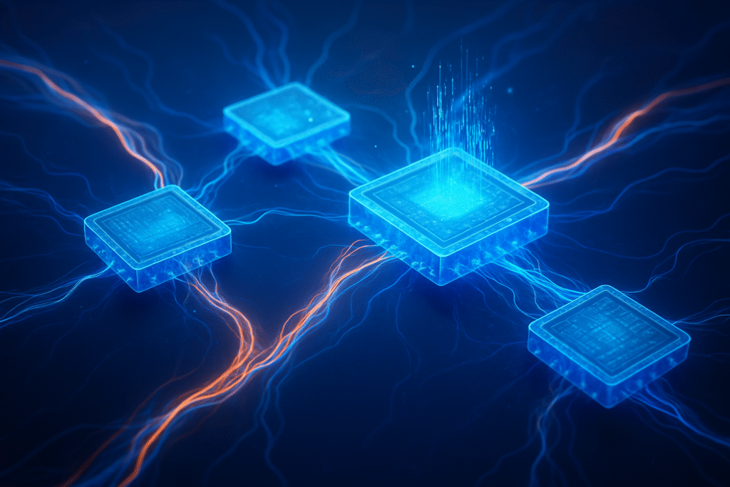
Chiplets are essentially small, specialized integrated circuits (ICs) that perform specific, well-defined functions. Instead of integrating all functionalities onto a single, large piece of silicon (a monolithic die), chiplets break down these functionalities into smaller, independently optimized dies. These individual chiplets — which could include CPU cores, GPU accelerators, memory controllers, or I/O interfaces — are then interconnected within a single package to create a more complex system-on-chip (SoC) or multi-die design. This approach is often likened to assembling a larger system using "Lego building blocks."
The functionality of chiplets hinges on three core pillars: modular design, high-speed interconnects, and advanced packaging. Each chiplet is designed as a self-contained unit, optimized for its particular task, allowing for independent development and manufacturing. Crucial to their integration are high-speed digital interfaces, often standardized through protocols like Universal Chiplet Interconnect Express (UCIe), Bunch of Wires (BoW), and Advanced Interface Bus (AIB), which ensure rapid, low-latency data transfer between components, even from different vendors. Finally, advanced packaging techniques such as 2.5D integration (chiplets placed side-by-side on an interposer) and 3D integration (chiplets stacked vertically) enable heterogeneous integration, where components fabricated using different process technologies can be combined for optimal performance and efficiency. This allows, for example, a cutting-edge 3nm or 5nm process node for compute-intensive AI logic, while less demanding I/O functions utilize more mature, cost-effective nodes. This contrasts sharply with previous approaches where an entire, complex chip had to conform to a single, often expensive, process node, limiting flexibility and driving up costs. The initial reaction from the AI research community and industry experts has been overwhelmingly positive, viewing chiplets as a critical enabler for scaling AI and extending the trajectory of Moore's Law.
Reshaping the AI Industry: A New Competitive Landscape
Chiplet technology is profoundly reshaping the competitive landscape for AI companies, tech giants, and startups alike. Major tech giants are at the forefront of this shift, leveraging chiplets to gain a strategic advantage. Companies like Advanced Micro Devices (NASDAQ: AMD) have been pioneers, with their Ryzen and EPYC processors, and Instinct MI300 series, extensively utilizing chiplets for CPU, GPU, and memory integration. Intel Corporation (NASDAQ: INTC) also employs chiplet-based designs in its Foveros 3D stacking technology and products like Sapphire Rapids and Ponte Vecchio. NVIDIA Corporation (NASDAQ: NVDA), a primary driver of advanced packaging demand, leverages chiplets in its powerful AI accelerators such as the H100 GPU. Even IBM (NYSE: IBM) has adopted modular chiplet designs for its Power10 processors and Telum AI chips. These companies stand to benefit immensely by designing custom AI chips optimized for their unique workloads, reducing dependence on external suppliers, controlling costs, and securing a competitive edge in the fiercely contested cloud AI services market.
For AI startups, chiplet technology represents a significant opportunity, lowering the barrier to entry for specialized AI hardware development. Instead of the immense capital investment traditionally required to design monolithic chips from scratch, startups can now leverage pre-designed and validated chiplet components. This significantly reduces research and development costs and time-to-market, fostering innovation by allowing startups to focus on specialized AI functions and integrate them with off-the-shelf chiplets. This democratizes access to advanced semiconductor capabilities, enabling smaller players to build competitive, high-performance AI solutions. This shift has created an "infrastructure arms race" where advanced packaging and chiplet integration have become critical strategic differentiators, challenging existing monopolies and fostering a more diverse and innovative AI hardware ecosystem.
Wider Significance: Fueling the AI Revolution
The wider significance of chiplet technology in the broader AI landscape cannot be overstated. It directly addresses the escalating computational demands of modern AI, particularly the massive processing requirements of LLMs and generative AI. By allowing customizable configurations of memory, processing power, and specialized AI accelerators, chiplets facilitate the building of supercomputers capable of handling these unprecedented demands. This modularity is crucial for the continuous scaling of complex AI models, enabling finer-grained specialization for tasks like natural language processing, computer vision, and recommendation engines.
Moreover, chiplets offer a pathway to continue improving performance and functionality as the physical limits of transistor miniaturization (Moore's Law) slow down. They represent a foundational shift that leverages advanced packaging and heterogeneous integration to achieve performance, cost, and energy scaling beyond what monolithic designs can offer. This has profound societal and economic impacts: making high-performance AI hardware more affordable and accessible, accelerating innovation across industries from healthcare to automotive, and contributing to environmental sustainability through improved energy efficiency (with some estimates suggesting 30-40% lower energy consumption for the same workload compared to monolithic designs). However, concerns remain regarding the complexity of integration, the need for universal standardization (despite efforts like UCIe), and potential security vulnerabilities in a multi-vendor supply chain. The ethical implications of more powerful generative AI, enabled by these chips, also loom large, requiring careful consideration.
The Horizon: Future Developments and Expert Predictions
The future of chiplet technology in AI is poised for rapid evolution. In the near term (1-5 years), we can expect broader adoption across various processors, with the UCIe standard maturing to foster greater interoperability. Advanced packaging techniques like 2.5D and 3D hybrid bonding will become standard for high-performance AI and HPC systems, alongside intensified adoption of High-Bandwidth Memory (HBM), particularly HBM4. AI itself will increasingly optimize chiplet-based semiconductor design.
Looking further ahead (beyond 5 years), the industry is moving towards fully modular semiconductor designs where custom chiplets dominate, optimized for specific AI workloads. The transition to prevalent 3D heterogeneous computing will allow for true 3D-ICs, stacking compute, memory, and logic layers to dramatically increase bandwidth and reduce latency. Miniaturization, sustainable packaging, and integration with emerging technologies like quantum computing and photonics are on the horizon. Co-packaged optics (CPO), integrating optical I/O directly with AI accelerators, is expected to replace traditional copper interconnects, drastically reducing power consumption and increasing data transfer speeds. Experts are overwhelmingly positive, predicting chiplets will be ubiquitous in almost all high-performance computing systems, revolutionizing AI hardware and driving market growth projected to reach hundreds of billions of dollars by the next decade. The package itself will become a crucial point of innovation, with value creation shifting towards companies capable of designing and integrating complex, system-level chip solutions.
A New Era of AI Hardware
Chiplet technology marks a pivotal moment in the history of artificial intelligence, representing a fundamental paradigm shift in semiconductor design. It is the critical enabler for the continued scalability and efficiency demanded by the current and future generations of AI models. By breaking down the monolithic barriers of traditional chip design, chiplets offer unprecedented opportunities for customization, performance, and cost reduction, effectively addressing the "memory wall" and other physical limitations that have challenged the industry.
This modular revolution is not without its hurdles, particularly concerning standardization, complex thermal management, and robust testing methodologies across a multi-vendor ecosystem. However, industry-wide collaboration, exemplified by initiatives like UCIe, is actively working to overcome these challenges. As we move towards a future where AI permeates every aspect of technology and society, chiplets will serve as the indispensable backbone, powering everything from advanced data centers and autonomous vehicles to intelligent edge devices. The coming weeks and months will undoubtedly see continued advancements in packaging, interconnects, and design methodologies, solidifying chiplets' role as the cornerstone of the AI era.
This content is intended for informational purposes only and represents analysis of current AI developments.
TokenRing AI delivers enterprise-grade solutions for multi-agent AI workflow orchestration, AI-powered development tools, and seamless remote collaboration platforms.
For more information, visit https://www.tokenring.ai/.
The current date is October 4, 2025.